Time:2013-06-02ClickTimes:
Jing-Jing Chen, Jie Meng, Yang-Bo Zhou, Han-Chun Wu, Ya-Qing Bie, Zhi-Min
Liao& Da-Peng Yu
1 State Key Laboratory for Mesoscopic Physics, Department of Physics, Peking
University, Beijing 100871, China.
2 CRANN and School of Physics, Trinity, College Dublin, Dublin 2, Ireland.
Graphene has various potential applications owing to its unique electronic,
optical, mechanical and chemical properties, which are primarily based on its
two-dimensional nature. Graphene-based vertical devices can extend the
investigations and potential applications range to three dimensions, while
interfacial properties are crucial for the function and performance of such
graphene vertical devices. Here we report a general method to construct
graphene vertical devices with controllable functions via choosing different
interfaces between graphene and other materials. Two types of vertically
conducting devices are demonstrated: graphene stacks sandwiched between two Au
micro-strips, and between two Co layers. The Au|graphene|Au junctions exhibit
large magnetoresistance with ratios up to 400% at room temperature, which have
potential applications in magnetic field sensors.
The Co|graphene|Co junctions display a robust spin valve effect at room
temperature. The layer-by-layer assembly of graphene offers a new route for
graphene vertical structures.
|
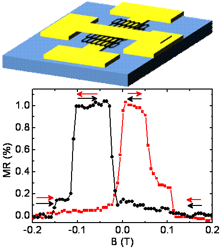
Transport properties of vertically conducting Au|graphene|Au
with deposited top Au electrode. (Uppera). Schematic diagram for the
Au/graphene/Au junction, where the top Au electrode was fabricated
via the processes including EBL, metal deposition and lift-off.
(Lower). Spin valves of Co/graphene/Co vertical structures.
|