Optimizing the electronic structures and carrier dynamics in semiconductors
at atomic scale is an essential issue for innovative device applications and
improving their functions, especially important for the micro/nano-scale
optoelectronic devices.The previous investigations of Prof. Dapeng Yu in School
of Physics have demonstrated that, due to the much higher elastic strain in
micro/nano-scale materials than their bulk counterpart (Physical Review B 73,
235409, 2006), the stain effect of semiconductors would be magnified at micro/nano-scale
(Advanced Materials 21, 4937, 2009), and the strain gradient may play an
important role in micro/nano-scale semiconductors (Advanced Materials
24,4707,2012). Therefore, elastic strainhas been proposed as a possible knob to
tailor the electronic structure and carrier dynamics in semiconductors.Recently,
major progresses have been achieved on elastic strain engineered semiconductor
micro/nano-structures.However, how does the elastic inhomogeneous strain field
influence the carrier dynamics in semiconductors is still elusive and a big
challenge due to the difficulty in precisely creating and controlling an elastic
inhomogeneous strain field in micro/nano-structures and the lack of an powerful
experimental characterization technique with enough spatial and temporal
resolutions.
Most recently, the Ph.D student Xuewen Fu and associate Prof. Zhimin Liao
etc. in Prof. Dapeng Yu’s group, which is affiliated with the National State Key
Laboratory of ‘Artificial Microstructure and MesoscopicPhysics’, and
Collaborative Innovation Centerof Quantum Material Science, have achieved great
progresses in tailoring exciton and carrier dynamics of semiconductors via
elastic strain gradient. They designed the experiment elaborately and realized
the standard 4-point-bending test on ZnOmico/nanowires for the first, then
throughthe careful continue-wave cathodoluminescence (CW-CL) measurements on the
purely bent ZnO micro/nanowires at low temperature (5.5 K), an abnormal over-all
redshift of up to 60 meV was observed at the whole pure bending cross. They
carried out collaboration with Prof. Ji Feng in the International Center of
Quantum Materialsat Peking University, Prof. Ju Li at MIT and Prof. WanlinGuo at
Nanjing University of Aeronautics and Astronautics, based on the theoretic
analysis and model numerical simulation, they proposedthat the abnormal
experimental phenomenon above is due to the elastic strain gradient driving
effect on theexcitons. These results werepublishedon one of the top journals in
the field of Nanomaterials and Nanoscience: Advanced Materials (Advanced
Materials 2014, 26, 2572, Xuewen Fu, et al.) on January 27.

|

|

|
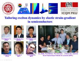
The authors and collaborators of this work
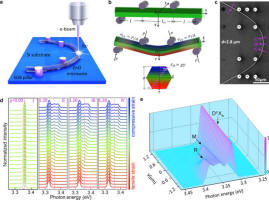
| a and b,Schematic diagram of CL measurement and strain distribution in a
4PBZnO MW; c, SEM image of a standard 4-point-bending ZnOmicrowire; d,
Line-scanning CL spectra of the 4-point-bending ZnOmicrowire;e,3-dimensional
image of the line-scanning CL spectra along the pure bending cross。
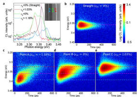
| a, The time-integrated CL spectra with pulsed electron beam exciting at
points A, B and C in the pure bending cross; b-e, The streak-camera images
showing emission energy as a function of time (the intensity being colour coded)
after pulsed electron excitation the straight part (b), points A, B and C of the
purely bent section (c,d,e).
|
After that, in order to confirm and observe theexciton drift effect under
elastic strain gradient by experiment directly, Mr. Xuewen Fu has been sent to
EPFL in Switzerland for half a year and carried collaboration with Prof. Benoit
Deveaud’s group. By using the unique time resolved cathodoluminescence (TRCL)
setup with both high spatial and temporal resolutions in EPFL, they further
carried out investigation on the picosecond resolved exciton dynamics of purely
bent ZnO micro/nanowires and directly observed the elastic strain gradient
driving effect on the excitons, demonstrating the important role of strain
gradient effect in semiconductors, i.e. the strain gradient can be effectively
used to tunetheexciton and carrier dynamics in semiconductors. It has great
guiding significance forthedevelopment of new kind semiconductor optoelectronic
devices. These results were published on another top journal in the field of
Nanomaterials and Nanoscience: ACS Nano (ACS Nano 2014, 8 (4), 3412. Xuewen Fu,
et al.)onMarch21. This work is a significant breakthrough in the area of
semiconductor exciton and carrier dynamics via high spatial and temporal
resolution investigation, and is alsothe unique report in this field in China.
Prof. Ji Feng in the International Center of Quantum Materials at Peking
University and Prof. WanlinGuo at Nanjing University of Aeronautics and
Astronautics, have done great theoretic contributions to this work.
This work was supported by National Natural Science Foundation, China/Swiss
Cooperation Project, National 973 Program, National State Key Laboratory of
‘Artificial Microstructure and Mesoscopic Physics’, and Collaborative Innovation
Center of Quantum Material Science.
