Tunable and sizable band gap of single-layer graphene sandwiched between hexagonal boron nitride
Time:2012-02-27ClickTimes:
Since its high carrier mobility (15000 cm2/V•s) on the SiO2 substrate at room temperature (one order of magnitude larger than that of Silicon), graphene is most likely to be applied in the new generation of high-performance electronics. However, pure graphene is a zero-bandgap semiconductor and thus cannot be directly used for effective room temperature field effect transistors (FET). Opening a tunable bandgap while keeping the high mobility of graphene at the same time is one of the most important and urgent topics in the graphene research currently.
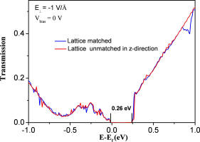
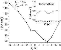
Recently, Prof. Jing Lu and Zhengxiang Gao from the Nano Physics Group at School of Physics, Peking University proposed a solution: insert the graphene between two hexagonal boron nitride (h-BN) sheets to form an h-BN/graphene/h-BN sandwich structure. The atomically flat h-BN substrate is helpful in improving carrier mobility because it is free from dangling bonds, which can reduce the irregularity, self-doping and chemical activity. Moreover, the h-BN and graphene is basically lattice matched but different in chemical potential. The symmetry between the two sublattice in graphene will be broken when graphene is sandwiched between the two h-BN sheets. A bandgap of 0.16 eV is opened for the h-BN/graphene/h-BN sandwich in a proper stacking mode. Applying a strong vertical electric field, the bandgap can increase to 0.34 eV. When the many-body effects are included, the zero-field band gaps are increased by more than 50% and thus can meet the practical logic device demands. By calculating the effective mass, they find that the high mobility of graphene can still be kept while the bandgap is opened in the sandwich structure. The ab initio quantum transport simulation of a dual-gated FET made of such a sandwich structure reveals an electric-field-enhanced transport gap, and the on/off current ratio is increased by a factor of 8.0 compared with that of a pure single layer graphene FET. Theoretically, the h-BN/graphene/h-BN sandwich structure is currently one of the most effective methods to continuously tune the bandgap and keep the high mobility of graphene at the same time. Relative work has been published on Nature Asia Materials (http://www.nature.com/am/journal/v4/n2/full/am201210a.html). Ruge Quhe and Jiaxin Zheng from Academy for Advanced Interdisciplinary Studies, Peking University and Guangfu Luo from Institute for Molecular Science, Japan contribute equally to this paper. The coworkers include Prof. Dapeng Yu (School of Physics, Peking University), Shigeru Nagase (Department of Theoretical and Computational Molecular Science, Institute for Molecular Science, Japan) and Wai-Ning Mei (Department of Physics, University of Nebraska at Omaha, USA).

|

|

|
FigureThe dual-gated field effect transistor based on the h-BN/graphene/h-BN sandwich structure. (Top) Schematic model,
(Left down) transmission spectrum, and (Right down) transfer characteristic under electric field of -1 V/Å.
Inset: transmission spectrum of single-layer graphene at zero bias.
|
This work was supported by the NSFC, National 973 Projects, Program for New Century Excellent Talents in University of MOE, NSFC, and State Key Laboratory of Mesoscopic Physics and Department of Physics, Peking University.
